Edge Capture Register
📌 Introduction
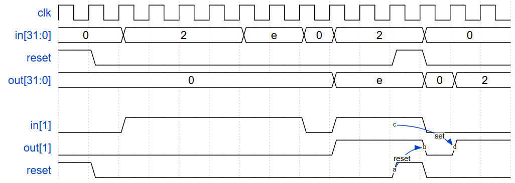
For each bit in a 32-bit vector, capture when the input signal changes from 1 in one clock cycle to 0 the next. “Capture” means that the output will remain 1 until the register is reset (synchronous reset).
Each output bit behaves like a SR flip-flop: The output bit should be set (to 1) the cycle after a 1 to 0 transition occurs. The output bit should be reset (to 0) at the positive clock edge when reset is high. If both of the above events occur at the same time, reset has precedence. In the last 4 cycles of the example waveform below, the ‘reset’ event occurs one cycle earlier than the ‘set’ event, so there is no conflict here.
🧑💻 Code Example
module top_module (
    input clk,
    input reset,
    input [31:0] in,
    output reg [31:0] out
);
    reg [31:0] pre;
    wire [31:0] falling_edge = pre & ~in;
    always @ (posedge clk) begin
        if (reset) begin
            out <= 32'd0;
            pre <= 32'd0;
        end
        else begin
        	out <= (out | falling_edge);
        end
        pre <= in;
    end

endmodule
In practical RTL design (especially for ASIC), it’s better to avoid using
initialto initialize registers and instead rely on a synchronous or asynchronous reset.
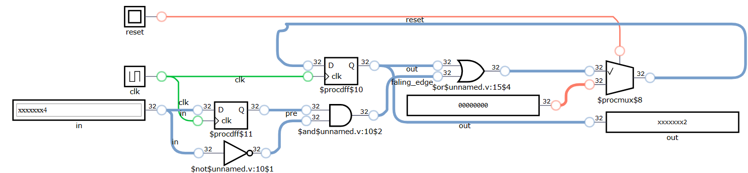
🧩 Block Diagram
This section visualizes the synthesized structure of the design through different tools.
DigitalJS shows a simplified gate-level representation, while Quartus provides RTL and
technology-mapped views based on actual FPGA implementation.
More Info ref Quartus Block Diagrams: RTL View & Technology Map
🔷 DigitalJS Logic Diagram
A high-level structural view automatically generated by DigitalJS.
🟦 Quartus RTL View
The RTL View is based directly on Verilog code.
It shows modules, registers, and logic before technology mapping.
🟩 Quartus Technology Map
Technology mapping shows how the design is implemented using FPGA logic elements (LEs),
including LUTs, registers, and routing structures.
📄 Technology Map – Post Mapping
📄 Technology Map – Post Fitting