3-input LUT (HDLBits)
8x1 Memory Circuit (Shift-in Write & Random-access Read)
📌 Question
In this question, you will design a circuit for an 8x1 memory, where writing to the memory is accomplished by shifting-in bits, and reading is “random access”, as in a typical RAM. You will then use the circuit to realize a 3-input logic function.
First, create an 8-bit shift register with 8 D-type flip-flops. Label the flip-flop outputs from Q[0]…Q[7]. The shift register input should be called S, which feeds the input of Q[0] (MSB is shifted in first). The enable input controls whether to shift. Then, extend the circuit to have 3 additional inputs A,B,C and an output Z. The circuit’s behaviour should be as follows: when ABC is 000, Z=Q[0], when ABC is 001, Z=Q[1], and so on. Your circuit should contain ONLY the 8-bit shift register, and multiplexers. (Aside: this circuit is called a 3-input look-up-table (LUT)).
Block Diagram Draw by GEMINI
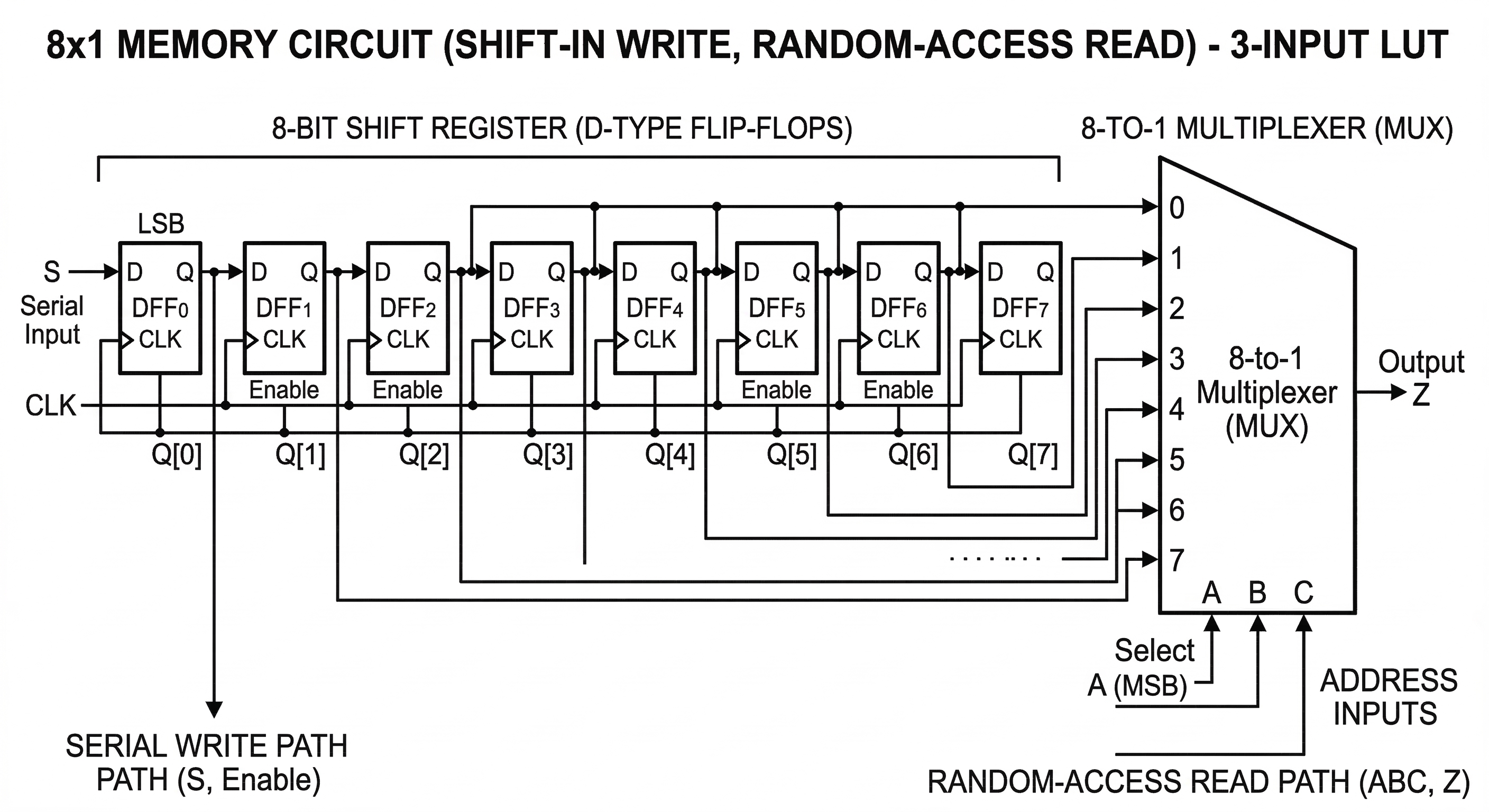
Although details not correct, it still can help us understand the question.
🧑💻 Code Example
You can also view my Github repo to see the whole project files, include below source code.
Brandon-git-hub/Open_EDA_Example - “3-input LUT (HDLBits)”
RTL Code
module top_module (
    input clk,
    input enable,
    input S,
    input A, B, C,
    output Z
);

genvar i;
wire [7:0] Q;

generate
    for (i=0; i<=7; i = i+'d1) begin: MEMORY_CIRCUIT
        EN_DFF dff(.clk(clk), .SI((i==0)? S: Q[i-1]), .enable(enable), .SO(Q[i]));
    end
endgenerate

wire [2:0] ACCESS_SEL;
assign ACCESS_SEL = {A, B, C};

assign Z = Q[ACCESS_SEL];

endmodule


module EN_DFF (
    input wire clk,
    input wire SI,
    input wire enable,
    output reg SO
);
    always @(posedge clk) begin
        if (enable) begin
            SO <= SI;
        end
    end
endmodule
Testbench Code
`timescale 1ns/1ps

module tb_top_module;

    // Inputs
    reg clk;
    reg enable;
    reg S;
    reg A, B, C;

    // Outputs
    wire Z;

    // Instantiate the Unit Under Test (UUT)
    top_module dut (
        .clk(clk),
        .enable(enable),
        .S(S),
        .A(A),
        .B(B),
        .C(C),
        .Z(Z)
    );

    initial begin
        clk = 0;
        forever #5 clk = ~clk; // 10ns period
    end

    initial begin
        $dumpfile("tb_top_module.vcd");
        $dumpvars(0, tb_top_module);

        // Initialize Inputs
        enable = 0;
        S = 0;
        A = 0;
        B = 0;
        C = 0;

        // Wait for global reset or startup
        #10;
        enable = 1;
        #80;
        S = 1;
        #10;
        S = 0;
        #70
        enable = 0;
        #30
        A = 1;
        B = 1;
        C = 1;
        #10
        A = 0;
        B = 0;
        C = 0;
        #10

        $finish;
        $display("Done.");
    end

endmodule
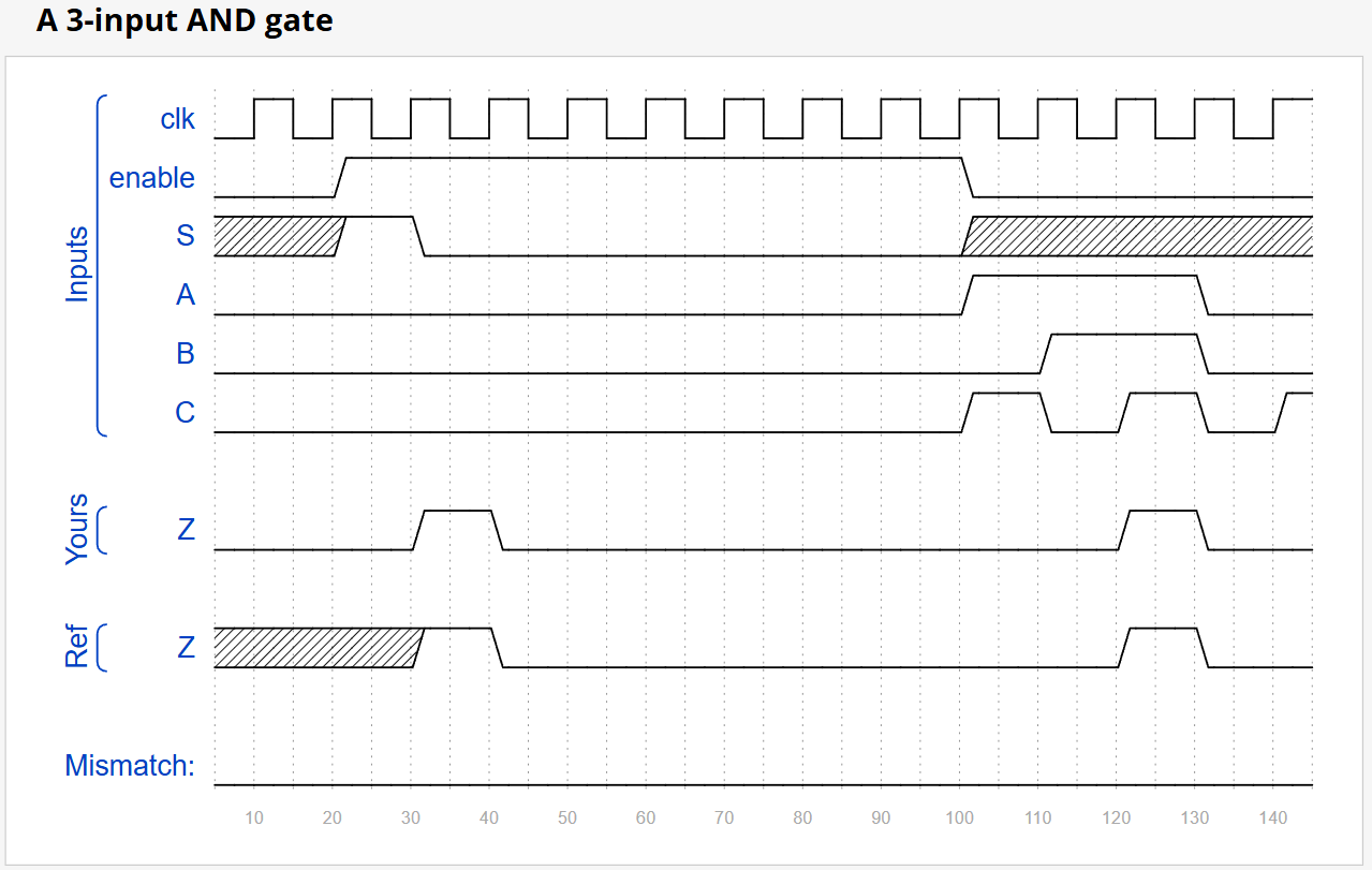
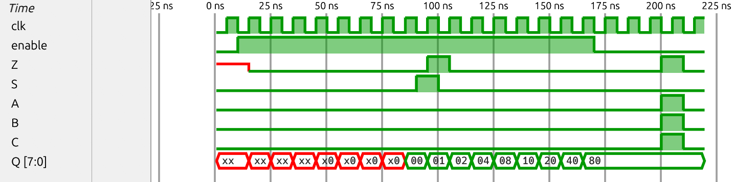
🔬 Results
Simulation Waveform
Synthesis RTL-level Schematic

Synthesis Gate-level Schematic

HDLBits Simulation Waveform